TSMC 2nm Update: N2 In 2025, N2P Loses Backside Power, and NanoFlex Brings Optimal Cells
by Anton Shilov on April 25, 2024 8:30 AM EST- Posted in
- Semiconductors
- TSMC
- 2nm
- N2
- Nanosheet
- N2P
- TSMC Symposium 2024
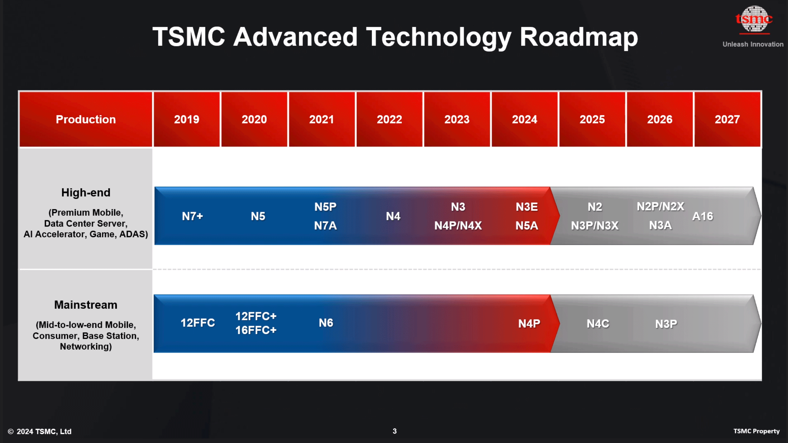
Taiwan Semiconductor Manufacturing Co. provided several important updates about its upcoming process technologies at its North American Technology Symposium 2024. At a high level, TSMC's 2 nm plans remain largely unchanged: the company is on track to start volume production of chips on it's first-generation GAAFET N2 node in the second half of 2025, and N2P will succeed N2 in late 2026 – albeit without the previously-announced backside power delivery capabilities. Meanwhile, the whole N2 family will be adding TSMC's new NanoFlex capability, which allows chip designers to mix and match cells from different libraries to optimize performance, power, and area (PPA).
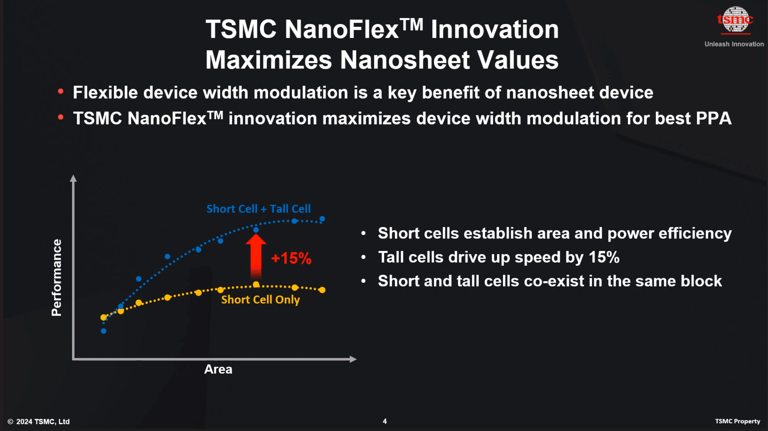
One of the key announcements of the event is TSMC's NanoFlex technology, which will be a part of the company's complete N2 family of production nodes (2 nm-class, N2, N2P, N2X). NanoFlex will enable chip designers to mix and match cells from different libraries (high performance, low power, area efficient) within the same block design, allowing designers to fine tune their chip designs to improve performance or lower power consumption.
TSMC's contemporary N3 fabrication process already supports a similar capability called FinFlex, which also allows designers to use cells from different libraries. But since N2 relies on gate-all-around (GAAFET) nanosheet transistors, NanoFlex gives TSMC some additional controls: firstly, TSMC can optimize channel width for performance and power and then build short cells (for area and power efficiency) or tall cells (for up to 15% higher performance).
When it comes to timing, TSMC's N2 is set to enter risk production in 2025 and high-volume manufacturing (HVM) in the second half of 2025, so it looks like we are going to see N2 chips in retail devices in 2026. Compared to N3E, TSMC expects N2 to increase performance by 10% to 15% at the same power, or reduce power consumption by 25% to 30% at the same frequency and complexity. As for chip density, the foundry is looking at a 15% density increase, which is a good degree of scaling by contemporary standards.
N2 will be followed by performance-enhanced N2P, as well as the voltage-enhanced N2X in 2026. Although TSMC once said that N2P would add backside power delivery network (BSPDN) in 2026, it looks like this will not be the case and N2P will use regular power delivery circuitry. The reason for this is unclear, but it looks like the company decided not to add a costly feature to N2P, but to reserve it to its next-generation node, which will also be available to customers in late 2026.
N2 is still expected to feature a major innovation related to power: super-high-performance metal-insulator-metal (SHPMIM) capacitors, which are are being added to improve power supply stability. The SHPMIM capacitor offers more than twice the capacity density of TSMC's existing super-high-density metal-insulator-metal (SHDMIM) capacitor. Additionally, the new SHPMIM capacitor cuts sheet resistance (Rs in Ohm/square) and via resistance (Rc) by 50% compared to its predecessor.
Related Reading
- TSMC's 1.6nm Technology Announced for Late 2026: A16 with "Super Power Rail" Backside Power
- TSMC Preps Cheaper 4nm N4C Process For 2025, Aiming For 8.5% Cost Reduction
- TSMC's System-on-Wafer Platform Goes 3D: CoW-SoW Stacks Up the Chips
- TSMC Jumps Into Silicon Photonics, Lays Out Roadmap For 12.8 Tbps COUPE On-Package Interconnect


0 Comments
View All Comments